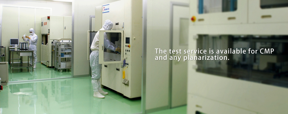
Please contact us if you are interested in CMP or wafer thinning process for semiconductor devices, brittle material, amorphous material, thin film, metal etc.

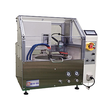
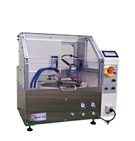
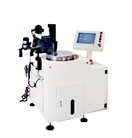
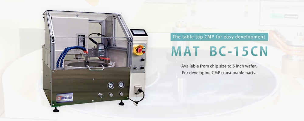
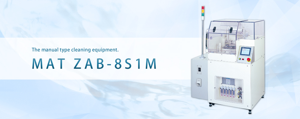
*Basic structure
*High rigidity
*Good cost performance
*Safety cover is equipped
*Demonstration is available
Kemet Japan Co., Ltd. can propose fine planarization; minimize surface profiling and thinning for next generation device with a lot of experience and unique technology.
Kemet Japan Co., Ltd. can provide test service for not only semiconductor but also SiC, GaN, MEMS, fine ceramics, LED, sapphire, organic EL etc.
The customer’s requirement such as target accuracy, through put, process steps, and budget will be discuss to promote the solution.
Kemet Japan Co., Ltd. also can propose test service for the development of consumable material such as polishing pad, polishing slurry, chemical cleaning, and grinding wheel.
For the equipment maintenance, we can offer the highly quality of flatness for platen, CMP head, and substrate using accurate lapping systems.
| Company name | Kemet Japan Co., Ltd. |
|---|---|
| President | Satoshi Takikawa |
| Head office Technical Lab1 |
Nakase Mihama-ku, Chiba City 2-6 WBG Malibu West 21F |
| TEL | +81-43-213-9911 |
| FAX | +81-43-213-9932 |
| Established | June 2002 |
| Capital stock | 32,000,000 |
| Business | Machine design and sales(Lapping and Polishing machine, Automated systems, Inspection system) Lapping and polishing tools design and sales. Consumable items for Lapping and Polishing sales. Lapping and Polishing services. |