
テスト加工PROCESS
TSVウエハ作製 CMP・Grind技術・加工装置
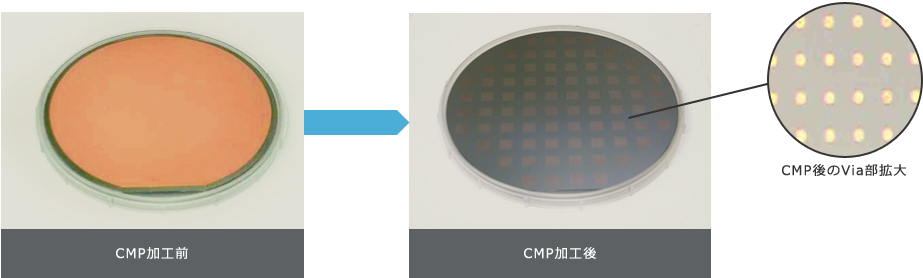
CMPにてViaトップの平坦化CMP: via top planarization.

Back grindとCMPで裏面側平坦化Grind and CMP: botttom planarization.

Via形成後Back grindとCMPで平坦化Grind and CMP: after via process

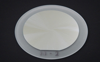
成膜後CMPで平坦化CMP: after plating process

表面粗さ向上CMP加工技術
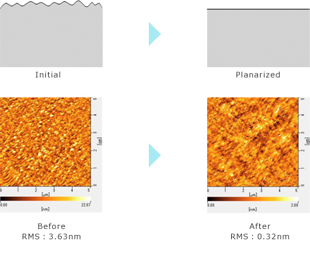
V接合面をCMPにて面粗さ向上CMP: Roughness control before wafer bonding
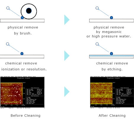
CMP後洗浄工程Cleaning process before wafer bonding
SiCウエハ研削技術のご提案
SiC ウエハ加工プロセス
①特殊砥石で高面粗度研削加工 ◎As Grind Ra ≦1.0nm
②特殊スラリーで研磨加工 ◎As Polish Ra ≦0.1nm
薄片・薄膜化 加工技術の紹介
MAT薄片・薄膜加工プロセスの特長MAT wafer thinning process
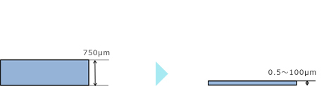
研削・研磨プロセスで、Si,Ge,glass,etcウエハを薄片・薄膜化が可能です。
研削
- ・単軸スピンドル構成なので砥石の変更が容易
- ・高番手砥石の使用でウエハを鏡面仕上げの研削プロセスが可能です
⇒研磨時間の短縮が可能 - ・1μm以下のTTVを実現
- ・Easy to change a grind wheel.
- ・Mirror finish by High mesh grinding wheel.
⇒ Reducing polishing process time. - ・Less than 1μm TTV.
研磨
- ・高性能CMPヘッドの仕様により、研削後のTTV形状の精度維持が可能
- ・工程ごとの部材選定が可能
⇒高スループットが実現
⇒薄片~薄膜化までのテスト加工ができます。
- ・High accuracy carrier heads
⇒ Reducing TTV deterioration. - ・Step process is available.
⇒ High productivity.
⇒ Available to make Thin Wf and Thin film